Aston™ 質譜分析儀應用於半導體蝕刻工藝瀏覽數: 1211
Aston™ 質譜分析儀應用於半導體蝕刻工藝
伯東公司日本 Atonarp Aston™ 質譜分析儀無等離子體設計, 可以實現快速, 化學特定的原位定量氣體分析, 與光學發射光譜 OES 對比, Aston™ 質譜儀的 OA% 靈敏度顯示為 <0.25%, 適用於半導體工藝中蝕刻計量控制, ALD, 3D-NAND 和新興的堆疊式 DRAM.
半導體蝕刻工藝挑戰日益增加
蝕刻是半導體製造中常用的工藝之一. 介電蝕刻用於形成絕緣結構, 觸點和通孔, 多晶矽蝕刻用於在電晶體中創建柵極, 金屬蝕刻去除材料以顯示電路連接圖案並鑽穿硬掩模.
Background: Increasing Challenges in Semiconductor Etch
Etch is one of the most frequently used processes in semiconductor manufacturing. While dielectric etch is employed to form insulating structures, contacts, and via holes, polysilicon etch is used to create the gate in a transistor, and metal etch removes material to reveal circuit connectivity patterning and drills through hard masks.
連續蝕刻鋁 Al, 鎢, 銅 Cu,鈦 Ti 和氮化鈦 TiN 等工藝金屬具有挑戰性, 因為許多金屬會形成非揮發性金屬鹵化物副產品(例如六氯化鎢 WCl6), 這些副產品會重新沉積在蝕刻側壁上, 導致成品率降低(通過微粒污染或沉積材料導致短路).
Continuous etching of process metals such as Aluminum(Al), Tungsten (W), Copper (Cu), Titanium (Ti), and Titanium Nitride (TiN) are often challenging, because many form non-volatile metal halide byproducts (e.g., tungsten hexachloride WCl6) that re-deposit on etched sidewalls resulting in lowered yield (through particulate contamination or deposited material causing electrical shorts).
隨著半導體行業不斷縮小關鍵特徵尺寸並採用垂直擴展 (如 3D-NAND 記憶體和全環繞柵極先進技術節點), 各種新的蝕刻挑戰已經出現. 這些包括在晶圓上蝕刻更小的特徵, 高展弦比 HAR 溝槽蝕刻 (具有小的開放面積百分比- OA%), 以及在新興的非揮發性記憶體和高 k介質中蝕刻金屬閘極, 稀土金屬等新材料. 對於先進的納米級工藝, 如蝕刻到矽介質和金屬薄膜, 選擇性處理, 如原子層蝕刻 ALE 一次去除材料的幾個原子層. ALE 提供了比傳統蝕刻技術更多的控制. 對於 3D-NAND 和先進 DRAM 來說, 向批量生產過渡的重大挑戰包括解決導體蝕刻困難的要求, 滿足積極的生產斜坡和實現所需的輸送量, 以推動成本效益.
A variety of new etch challenges have emerged as the semiconductor industry continues to shrink critical feature sizes and adopt vertical scaling e.g., in 3D-NAND memory and gate-all-around advanced technology nodes. These include etching smaller features, high aspect ratio (HAR) trench etch (with small open area percentage -OA%) on the wafer and etching new materials such as metal-gates, rare earth metals in emerging non-volatile memories and high-k dielectrics. For advanced process nanoscale features e.g. etch into silicon dielectrics and metal films, selective processing such as atomic layer etching (ALE) removes a few atomic layers of material at a time. ALE offers more control than conventional etch techniques. For both 3D-NAND and advanced DRAM, significant challenges in transitioning into volume production include addressing difficult conductor etch requirements, meeting aggressive production ramps and achieving the needed throughput to drive cost benefits.
伯東公司日本 Atonarp Aston™ 質譜分析儀提供高性能, 嵌入式和可靠的原位定量分子氣體計量已經成為驗證工藝室和持續監測工藝化學過程的關鍵工具, 確保生產環境中的高產率和更大輸送量.
High performance, embedded, and reliable in-situ quantitative molecular gas metrology have emerged as a crucial tool to qualify process chambers and continuously monitor process chemistries, all to ensure high yields and maximize throughput in production environments.
Aston™ 質譜分析儀提供全腔室解決方案
使用伯東 Atonarp Aston™ 質譜分析儀通過即時, 定量和精確的分子感測器來解決半導體新興蝕刻工藝技術相關的關鍵挑戰. 通過解決感測器耐久性, 靈敏度, 匹配, 系統集成和易用性等方面的挑戰, 日本 Atonarp Aston™ 質譜分析儀升級了傳統的氣體分析計量方法. Aston 是一種全室解決方案, 用於在各種工藝步驟中即時監測前體, 反應物和副產物.
Aston: A Total Chamber Solution
Atonarp’s Aston™ upgrades conventional gas analysis metrology by addressing challenges revolving around sensor durability, sensitivity, matching, system integration and ease-of-use. Aston is a total chamber solution for real time in-situ monitoring of precursors, reactants, and byproducts during various process steps.
這些包括基準室和過程指證, 腔室清潔, 過程監測 (包括存在腐蝕性氣體), 顆粒沉積和氣體污染物凝結. 小的占地面積和靈活的通信介面允許在室內安裝和集成到過程設備控制系統. 為了集成到半導體工藝工具中, Aston 質譜分析儀的高性能和可靠性設計用於生產晶圓的大批量生產程序控制.
These include baseline chamber and process fingerprinting, chamber clean, process monitoring (including in the presence of corrosive gases), particle deposition, and gaseous contaminant condensation. The small footprint and flexible communication interface allow for on-chamber installation and total integration into the process equipment control system. Intended for full integration into the process tool, Aston’s high performance and dependability are designed for high volume run-to-run process control of production wafers.
Aston™ 質譜分析儀半導體蝕刻計量控制
半導體行業正從二維結構的擴展轉向複雜三維結構的挑戰性要求. 傳統的離線晶圓測量已不足以實現性能和良率目標, 原位蝕刻測量傳統上缺乏生產所需的魯棒性和可重複性. Aston™ 質譜分析儀的結構中嵌入了專利技術, 使其具有卓越的分析和操作性能. 為了滿足程序控制和跨工廠生產工具匹配的嚴格要求, Aston 從頭開始設計, 高執行時間和低維護的輸送量, 長期信號穩定性和可重複性.
Measurement-Based Control
The semiconductor industry is shifting from scaling of 2Dstructures to the challenging requirement of complex 3D
structures. Conventional offline wafer metrology is no longer sufficient to achieve performance and yield goals and in-situ etch measurement has traditionally lacked the robustness and repeatability needed for production.
Embedded into the architecture of Aston™ are patented technologies enabling superior analytical and operational
performance. To meet the stringent requirements for process control and matching on production tools across
fab locations, Aston is designed from the ground up for high up-time and throughput with low maintenance, longterm signal stability, and repeatability.
為了承受腐蝕和沉積過程的惡劣環境, Aston™ 引入了兩個革命性的功能: 等離子電離和自清潔 (ReGen™模式). 等離子體電離消除了由於與腐蝕性氣體(如NF3, CF4, Cl2)的反應而導致的燈絲降解. 此外, 除去(正矽酸四乙酯) TEOS 等顆粒和蒸汽污染物沉積, 同時定期進行室內清潔迴圈, 延長了 Aston™ 質譜儀的使用壽命. ReGenTM 模式使儀器能夠使用高能等離子離子清洗自身, 通過去除在膜沉積過程中可能發生在感測器和腔室壁上的沉積. 結合這兩個功能, 感測器的靈敏度可維持在數百個RF(射頻)小時的操作. Aston質譜儀支持的基於測量的控制, 有可能延長清洗間隔 MTBC 的平均時間. MTBC 的增加意味著工具可用性和長期輸送量的增加. 除了等離子電離器(用於工藝), 感測器還配備了傳統的電子衝擊 EI 燈絲電離器, 用於基線和校準.
To withstand the harsh environment of etch and deposition processes, Aston™ introduces two revolutionary features: Plasma Ionization and selfcleaning (ReGen™ mode). Plasma ionization eliminates filament degradation due to reactivity with aggressive gases (e.g., NF3, CF4, Cl2). Additionally, the removal of particles such as (Tetraethyl Orthosilicate) TEOS and vapor contaminant deposits concurrently with regularly scheduled chamber clean cycles, give the Aston™ an extended lifetime. The ReGenTM mode enables the instrument to clean itself using energetic plasma ions, by removing deposits on the sensor and chamber walls that may occur during film deposition processes. Combined, these two features maintain sensor sensitivity over hundreds of RF (Radio Frequency) hours of operation. The measurement-based control enabled by Aston offers the potential to extend the mean time between cleans (MTBC). An increase in MTBC translates into an increase in tool availability and long-term throughput. In addition to the Plasma ionizer (for process), the sensor is outfitted with conventional electron impact (EI) filament ionizer, which is used for baselining and calibration.
分子感測器的分析級是使用微米級精密雙曲電極的四極杆. 由高度線性射頻(RF)電路驅動, Aston 質譜的 HyperQuad 感測器在 2到 300 amu的質量範圍內具有更高的分析性能.
The analytical stage of the molecular sensor is a quadrupole using micro-metre-level machined accurate hyperbolic electrodes. Driven by a highly linear Radio Frequency (RF) circuitry, Aston’s HyperQuad sensor produces superior analytical performance (Table 1.) over a mass range of 2 to 300 amu.
Aston™ 質譜分析儀技術參數
|
參數 Parameter |
值 Typical |
|
質量解析度 Mass resolution |
0.8u |
|
質量數穩定性 Mass number stability |
0.1u |
|
靈敏度 (FC / SEM) Sensitivity (FC/SEM) |
5x10⁻⁶ / 5x10⁻⁴ A/Torr |
|
最低可檢測的部分 Minimum detectable partial |
10-9 / 10-11 Torr |
|
檢測極限 Limit of Detection |
10 ppb |
|
最大工作壓力 Maximum operating pressure |
1X10⁻³ Torr |
|
每 u 停留時間 Dwell time per u |
40 ms |
|
每 u 掃描更新率 Scan update rate per u |
37 ms |
|
發射電流 Emission current |
0.4 mA |
|
發射電流精度 Emission current accuracy |
0.05 % |
|
啟動時間 Start-up time |
5mins |
|
離子電流穩定 Ion Current Stability |
< ±1% |
|
濃度的準確性 Concentration Accuracy |
< 1% |
|
濃度穩定 Concentration Stability |
±0.5% |
|
電力消耗 Power consumption |
350w |
|
重量 Weight |
13.7kg |
|
尺寸 Size |
400 x 297 x 341mm |
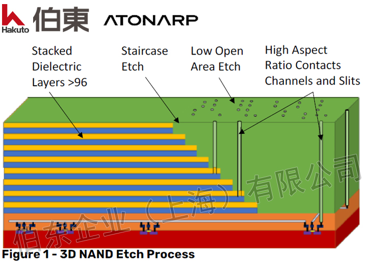
高展弦比 HAR 3D 蝕刻
隨著多模式技術和 3D器件結構的出現, 高度密集的蝕刻和沉積過程驅動了計量需求. 3D多層膜棧, 如 NAND 存儲架構, 代表複雜的, 具有挑戰性的蝕刻過程, 具有關鍵的蝕刻角度, 統一的通道直徑和形狀要求, 儘管高蝕刻縱橫比通道 >100:1 是常見的. 對於 3D-NAND, 關鍵導體蝕刻過程包括階梯蝕刻(下圖)和用於垂直通道和狹縫的 HAR 掩模打開. 通過硝酸矽和氧化矽交替層蝕刻需要高速定量終點檢測. 對於 DRAM, 蝕刻過程包括 HAR 門, HAR 溝槽和金屬隱窩. 對於階梯蝕刻, 關鍵是在整個 3D堆疊的每個介質膜對的邊緣創建等寬的“步驟”, 以形成階梯形狀的結構. 在器件加工過程中, 這些步驟的大量重複要求蝕刻高輸送量和嚴格的程序控制.
High Aspect Ratio (HAR) 3D-Etch
With the advent of multi-patterning technologies and 3D device structures, metrology requirements are driven by
highly intensive etch and deposition processes. 3D multilayer film stacks, such as NAND memory architectures,
represent complex, challenging etch processes with critical etch angle, uniform channel diameter and shape
required, despite high etch aspect ratio channels >100:1 being common. For 3D-NAND, critical conductor etch processes include staircase etch (figure 1) and HAR mask open for vertical channels and slit. Etching through
alternate layers of silicon nitrate and silicon oxide requires high speed quantitative end point detection. For DRAM, etch processes include HAR gates, HAR trenches and metal recess. For staircase etch, it is critical that equalwidth "steps" are created at the edge of each dielectricfilm pair throughout the 3D stack to form a staircaseshaped structure. Extensive repetition of these steps during device processing requires etching at high
throughput with stringent process control.
多功能現場氣體計量需要在一個工具中執行多種監測功能:
• 檢測和量化污染, 交叉污染, 氣體雜質和工藝室內的工藝化學
• 評估已開發的蝕刻過程在生產工具 / 運行的複雜功能上的性能
• 測量刻蝕後的清潔 (包括先進的無晶圓自動清潔; WAC) 作為腔條件對於消除工藝漂移和確保可重複性性能是至關重要的
• 快速準確的蝕刻端點檢測 EPD, 通過等離子體或氣體監測, 因為這是一個關鍵的控制功能. 舉例包括一氧化碳 CO 副產物在介電蝕刻中下降或氯 Cl 反應物在多晶矽和金屬蝕刻端點上升.
• 全面的即時計量資料, 允許過程等離子體和反應物的動態腐蝕控制, 以管理要求的腐蝕剖面
Versatile in-situ gas metrology is needed to perform multiple monitoring functions in a single tool:
• Detect and quantify contamination, crosscontamination, gas impurities and process chemistry inside the process chamber
• Assess performance of developed etch recipes on complex features on production tools/runs,
• Measure post-etch clean (including advanced waferless auto clean; WAC) as chamber condition is critical to eliminating process drifts and ensuring repeatable performance
• Rapid and accurate etch endpoint detection (EPD), through plasma or gas monitoring, as it is a critical control function. Examples include carbon monoxide (CO) byproducts decline in dielectric etching or Chlorine (Cl) reactants rise in polysilicon and metal etching at endpoint
• Comprehensive real-time metrology data to allow for dynamic etch control of process plasma and reactants to manage the demanding etch profiles
Aston™ 質譜分析儀無等離子體終點檢測
雖然光學發射光譜 OES 已被廣泛用於蝕刻 EPD, 但低開放面積 OA 和 HAR 設計的趨勢使其在許多蝕刻任務中無效. OES 技術需要等離子體'開'和發光物種. 隨著昏暗和遠端等離子體越來越多地用於 3D設備和原子水準蝕刻 ALE 工藝, 需要更多敏感的資料和分析技術來實現迅速和確定的 EPD. 此外, 脈衝等離子體通常用於管理 HAR 和 低 OA% 工藝的蝕刻剖面, 這使得 OES 對於 EPD 來說是一個不切實際的解決方案. 在3D 結構中, 多層薄膜和多個接觸深度阻礙了每一行觸點到達底部時端點的光學發射信號的急劇步進變化
End Point Detection without Plasma
While optical emission spectroscopy (OES) has been widely adopted for etch EPD, the trend for low open area
(OA) and HAR designs make it ineffective for many etch tasks. OES techniques require plasma ‘on’ and light
emitting species. More sensitive data and analysis techniques are required to achieve prompt and deterministic EPD as dim and remote plasmas are increasingly used in 3D devices and atomic level etch (ALE) processes. Further, pulsed plasma is often used to manage the etch profile in HAR and low OA% processes making OES an impractical solution for EPD. In 3D structures, multi-layer film and multiple contact depths hinder the ability to get a sharp step change in optical emission signal for endpoint as each row of contacts reaches the bottom.
其他 OES 限制包括:
• 在電介質蝕刻中, 在 OA <5% 的模式上進行 EPD一直具有挑戰性, 因為 OES 在低濃度下具有低信噪比.在高壓Si深蝕刻(例如博世工藝)中, 要求 OA% 的 EPD低於 0.3%, OES 中較大的背景雜訊水準抑制了對發射種數量的任何變化的檢測.
• 在金屬蝕刻中, OA% 可能低於10%, 這取決於所涉及的互連尺寸. 對於接觸和通過蝕刻, OA 可以在0.1-0.5%之間或更低, 這取決於所涉及的特徵的大小. 在鎢 W 蝕刻的情況下, 隨著 OA的減小, 氯 Cl 反應物的消耗減少, 由於材料運輸到 HAR 蝕刻特徵, 蝕刻趨於放緩. 這兩個因素都降低了反應氣的消耗率. 因此, 由於等離子體中反應物的耗盡, 很難看到在終點處 OES信號的顯著變化.
Other OES Limitations include:
• In dielectric etch EPD on patterns with <5% OA has always been challenging as OES has low signal to noise at low concentrations. In high pressure Si deep etch (i.e. Bosch process), where EPD for OA% under 0.3% is required, the large background noise level in OES inhibits detecting any changes in the amount of emitting species.
• In metal etches the OA% may be under 10% depending on the size of the inter-connects involved. For contact and via etches the OA can be between 0.1-0.5% or less depending on the size of the features involved. In the case of tungsten (W) etch, the consumption of chlorine (Cl) reactants decreases with smaller OA, and due to material transport into the HAR etch feature, the etch tends to slowdown. Both factors decrease the rate of consumption of reactant gas. Therefore, it is difficult to see a significant change in OES signal at endpoint due to depletion of reactants from the plasma.
Aston™ 質譜分析儀可以利用蝕刻反應物和 EPD 的副產物. 此外, Aston 能夠在小的, 有限體積的感測器上運行週期性清洗, 以保持其性能(靈敏度), 在延長晶圓運行次數的情況下獲得更大的正常執行時間. 然而, OES 要求在腔室上有一個需要保持清潔的訪問視窗,以獲得足夠強度的穩定信號。通常,加熱石英窗用於減緩工藝產品的堆積. 使用 Aston™質譜分析儀,在低濃度下的檢測不受等離子體發射的背景光譜的影響, 也不受射頻功率脈衝期間等離子體強度波動的影響.
圖 3a/3b 顯示了 CO+和 SiF3 +的副產物 OA%下降到 0.25%的電介質腐蝕 EPD 資料
Aston™ can utilize both etch reactants and byproducts for EPD. Furthermore, Aston is able to run a periodic clean on the small, confined volume of the sensor to maintain its performance (sensitivity) over extended number of wafer runs for maximum uptime. OES however, require an access window on the chamber that must remain clean to obtain stable signals of sufficient intensity. Typically, a heated quartz window is used to slow down buildup of process products. With Aston™, detection at low concentrations is not affected by either background light
spectrum being emitted by plasma nor fluctuations in plasma intensity during RF power pulsing.
Figures 3a/3b show dielectric etch EPD data as a function of OA% down to 0.25% for both CO+ and SiF3
+ byproducts.
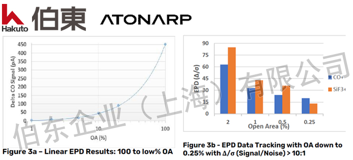
資料清楚地顯示了線性行為和在低濃度下的檢測不受等離子體發射的背景光譜影響. Aston 質譜的 ppb 靈敏度是針對 0.1%以下的 OA性能.
The data clearly shows a linear behavior and a detection at low concentrations not affected by background light spectrum being emitted by plasma. Sub 0.1% OA performance is targeted with Aston’s ppb sensitivity
原子級蝕刻 ALE
在三維結構中, ALE 過程中的逐層去除需要脈衝射頻電源來控制自由基密度和較低的離子能量, 以減少表面損傷和保持方向性. 在這樣的光源中, 等離子體的整體光強較低, 並表現出波動幅度. 通常等離子體離晶圓區很遠(>距晶圓區25釐米), 而且等離子體激發的副產物很少, 使得光學測量不切實際.
Atomic Level Etch (ALE)
In 3D structures, layer-by-layer removal in ALE processes require pulsed RF power sources to control radical
densities and lower ion energy to minimize surface damage and maintain directionality. In such sources, the plasma’s overall light intensity is lower and exhibits a fluctuating magnitude. Often the plasma is far away (> 25
cm separation from the wafer region) and so few byproducts are excited by the plasma making optical metrology impractical.

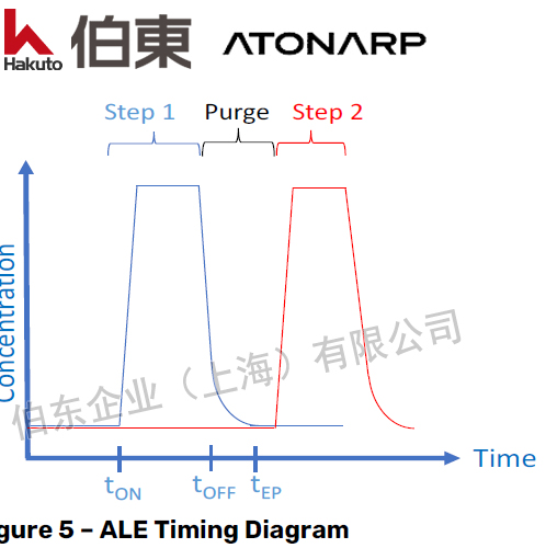
在 ALE中, 由於每個週期都是自我限制的, 端點檢測可能不那麼重要. 然而, 在缺乏氣體分析的情況下, 工藝工程師對監測腔室和工藝健康狀況“視而不見”, 因為無法看到化學狀態, 特別是在工藝步驟 (吸附/淨化/反應/淨化) 之間過渡時的動態狀態, ALE 的自限性並不能使它不受過程漂移的影響. 此外, 由於 ALE 不是基於等離子體的, 因此過程中的化學變化不一定可以通過等離子體監測檢測到.
In ALE, since each cycle is self-limiting, endpoint detection may not be as critical. However, in the absence of gas analysis, process engineers are “blind” to monitoring chamber and process health as there is no visibility to chemical state, especially the dynamic state when transitioning between process steps (adsorb / purge / react / purge) as shown on Figure 4. The selflimiting nature of ALE does not make it immune to process drifts. Furthermore, since ALE is not plasma-based, chemical changes in the process are not necessarily detected via plasma monitoring.
有一種誤解, 認為 ALE 技術實際上是一次一個原子層; 相反, 它們每迴圈的去除/沉積量可能比單分子膜多一點(或少一點). 由於真空泵性能, 晶圓溫度或離子轟擊能量 (電壓) 的變化分別導致表面飽和度和表面反應性的變化, 工藝移位(Å/週期的變化)可能發生.
There is a misconception that ALE techniques are truly one atomic layer at a time; rather, they have a characteristic removal/deposition amount per cycle which can be a little bit more than a monolayer (or a little less). Process shifts (change in Å/cycle) can occur due to changes in surface saturation and surface reactivity caused by changes in pumping performance, wafer temperature or ion bombardment energy (voltage) respectively.
在 ALE (下圖)中,由於等離子體的使用不一致, 化學監測方面的差距就不那麼明顯了. 在這種情況下, Aston™ 質譜儀具有以下優點:
• 在每個工藝步驟中建立一個腔室化學狀態的指證. 這可以參照其自身的正常行為, 也可以參照標準腔
• 描述和監控與化學變化相關的動態過程中, 從一個步驟過渡到下一個步驟
• 監測在 ALE 迴圈第一步之後從系統中清除吸附物質的時間. 等離子體通常用於產生吸附物質(自由基), 但它是在遠離晶圓片的地方產生的
• 監測 ALE 迴圈第二步反應產物的變化. 等離子體光強通常較低, 因為它使用了低占空比的脈衝射頻
• 監測反應產物和反應物在ALE迴圈第二步後被淨化的時間
In ALE (figure 5), since a plasma is not used consistently, the gaps in chemical monitoring are not as obvious. In such scenarios, Aston™ offers the following benefits:
• Develop a fingerprint of the chemical state of a chamber during each process step. This can be inreference
to its own normal behavior, or to a reference golden chamber
• Characterize and monitor the dynamics associated with chemical changes during the steps and when transitioning from one step to the next
• Monitor time for adsorbing species to be purged from the system after the first step of the ALE cycle (figure 5). The plasma is typically used to create adsorbing species (radicals), but it is created far from the wafer
• Monitor change in reaction product formed during the 2nd step of ALE cycle. The plasma optical intensity is typically low since it uses a low duty cycle pulsed RF
• Monitor time for reaction product and reactant to be purged after 2nd step of ALE cycle
結論
原子級蝕刻只能使用像上海伯東日本 Atonarp Aston™ 質譜分析儀這樣的分子感測器進行真正的測量和監測. 它的高靈敏度, 速度和對等離子體強度變化的低敏感性產生可靠的定量測量, 即使在低濃度的反應物和副產物, 具有低於1% 水準的高精度, 可以監測微妙的過程漂移和過程變化效應, 提供了可用於機器學習模型的見解.
Conclusion
Atomic level etch can only be truly measured and monitored using a molecular sensor device such as Aston™. Its high sensitivity, speed, and lower susceptibility to plasma intensity variations produce reliable quantitative measurements even with low concentrations of reactants and byproducts. With high accuracy at sub-1% levels, it can monitor subtle process drifts and process variation effects providing insights that can be used for machine learning models.
利用其高掃描速度, 通過監測反應產物減少的時間來實現步進時間優化, 因為它是表面反應活性變化的指示, 增加了總體輸送量.
Using its high scan speed, step-time optimization is achieved via monitoring of the time for reaction product
to decrease as it is an indication of a change in surface reactivity, increasing overall throughput.
ALE 是先進的蝕刻技術, 伯東 Aston™ 質譜分析儀為 ALE 提供了先進的化學計量技術, 可以測量和控制反應及其持續時間, 為大批量生產提供了可靠的解決方案.
ALE is the most advanced etch technique and it lies at the frontier of the ability to cost effectively manufacture advance semiconductor processes. Aston enables ALE advanced chemistry metrology, to measure and control reactions and their duration, providing a robust solution for high volume production.
若您需要進一步的瞭解 Atonarp Aston™ 在線質譜儀詳細資訊或討論, 請參考以下聯絡方式:
上海伯東: 葉小姐 臺灣伯東: 王小姐
T: +86-21-5046-3511 ext 107 T: +886-3-567-9508 ext 161
F: +86-21-5046-1490 F: +886-3-567-0049
M: +86 1391-883-7267 ( 微信同號 ) M: +886-975-571-910
qq: 2821409400
現部分品牌誠招合作代理商, 有意向者歡迎聯絡伯東 王小姐 +886-975-571-910
伯東版權所有, 翻拷必究
![]() +886-2-8772-8910
+886-2-8772-8910