Aston™ 質譜分析儀為 Sub-fab 提供安全, 可持續性發展的監測控制方案瀏覽數: 964
Aston™ 質譜分析儀為 Sub-fab 提供安全, 可持續性發展的監測控制方案
Sub-fab 一直是半導體製造設施的後端方案. 與 FAB 的主要加工走廊不同, Sub-fab 中的設備被歸入與基本工具管理和廢物處理相關的系統: 幹式真空泵, 燃燒和吸收器減排系統, 水處理器和冷卻器以及散裝材料的輸送和管理是 Sub-fab 設備執行的關鍵功能.
The Sub-fab has historically been somewhat of an afterthought in semiconductor fabrication facilities. Unlike the main processing corridors of the main FAB the equipment in the sub-fab is relegated to systems associated with basic tool management and waste handling: dry vacuum pumps, combustion and absorber abatement systems and water handler and chillers along with bulk materials delivery and management are come of the key functions sub-fab equipment performs.
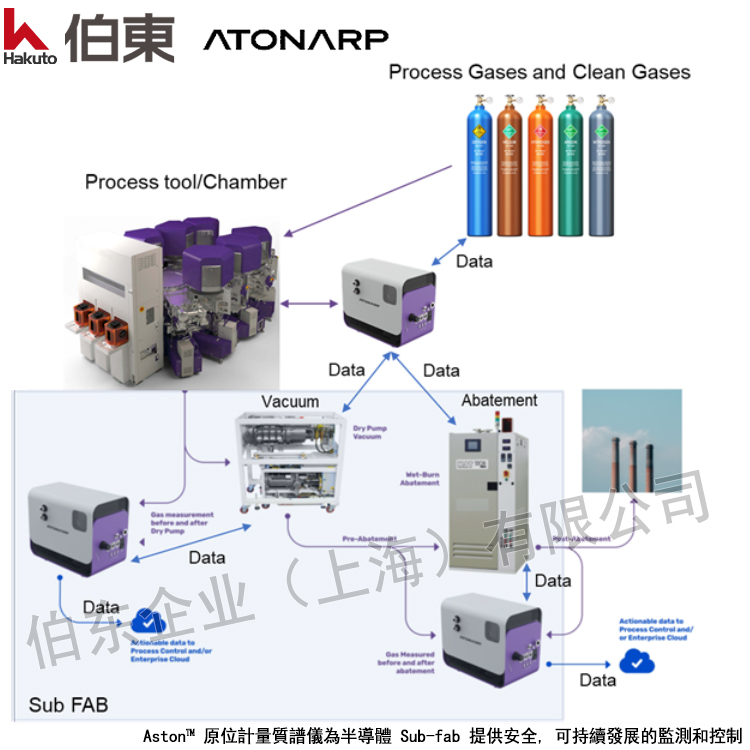
伯東公司日本 Atonarp Aston™ 質譜分析儀提供穩健, 量化和即時的計量. 原位量化計量在關鍵靈敏度 / 速度指標上比其他殘留氣體分析儀優於 10 倍至 100 倍, 並具有強大的等離子電離解決方案, 使它們能夠處理苛刻的工藝氣體和副產品. 為半導體 Sub-fab 提供安全, 可持續性和節約解決方案.
The common thread to Sub-FAB applications of safety, sustainability and savings is that to improve them you must measure and quantify the materials to be managed. There is a need for robust, quantified, and realtime metrology both on the chamber and as part of the sub-fab infrastructure. The Aston family of realtime semiconductor metrology solutions from Atonarp provide in-situ quantified metrology that is 10x to 100x better on the key sensitivity/speed metric than other residual gas analyzers with a robust plasma ionization solution that allows them to work with harsh process gases and by-products.
隨著半導體製造足跡對環境的影響對晶圓廠運營商變得越來越重要, 在客戶對更高可持續性的需求的推動下, Sub-fab 越來越被視為提高效率和可持續性的關鍵部分. 隨著對安全的普遍需求, 對可持續性和效率的額外關注正在推動重新關注使用即時現場監控和控制更智慧地運行 Sub-fab 設備.
However, as the impact that the semiconductor manufacture footprint has on the environment becomes increasing important to fab operators, driven by their clients demands for greater sustainability, the sub-fab is increasing seen as a critical part of driving efficiency and sustainability. Along with the omnipresent need for safety, the added focus on sustainability and efficiency is driving a renewed focus on running sub-fab equipment smarter using real-time in-situ monitor and control.
問題
Sub-fab 管理的三大支柱, 即安全性, 可持續性和節約性正在重新受到關注.
The three pillars of sub-fab management, namely: Safety, Sustainability and Savings are receiving renewed attention.
對於分子水準安全監測: 先進的工藝推動了對新型危險材料和副產品的需求, 對前沿邏輯工藝, 鑄造和記憶體工藝的需求不斷增加, 特別是在 ALD 和 ALE 中使用選擇性處理化學物質的情況下. 2019 年的一項研究表明, 在 2017 年 2019 年的 30 多起不良事件中, 包括爆炸, 火災, 放熱反應, 化學反應和排氣. 大多數事件發生在從腔室到減排系統的排氣處理路徑中的 Sub-fab 中.
For molecular Level Safety monitoring: Advanced processes are driving a need as new and hazardous materials and by products are increasing needed for leading edge logic, foundry, and memory processes especially where selective processing chemistry is used in ALD and ALE. A 2019 study showed that in greater than 30 adverse events in 2017-2019 include explosions, fires, exothermic reactions, chemical reactions, and off-gassing. Most events occurred in the sub-FAB in the exhaust handling pathway from the chamber through abatement systems.
目前使用分子安全監測的一些例子包括: 當爆炸鋯金屬顆粒是潛在的副產品時, 基於用於邏輯門和 DRAM 電容器結構的鋯的高k介電材料. 此外, 在快閃記憶體製造中用於氧化矽原子級沉積的高階矽烷化學對主動洩漏檢測提出了挑戰, 以防止需要監控和管理的產品氣體和冷凝物引起的火災和危險.
Some current examples where molecular safety monitoring is used would include: high-K dielectric materials based on Zirconium used for logic gates and DRAM capacitor constructs when explosive Zirconium metallic particles are a potential by product. Additionally high order silane chemistry used in atomic level deposition of silicon oxides in flash memory manufacturing present challenges with active leak detection to prevent fires and hazardous by product gases and condensates that need to be monitored and managed.
除了安全之外, 可持續性也是重點: 最近的研究表明, 超過 80% 的智慧手機碳足跡不是在使用過程中產生的, 而是在製造過程中產生的, 其中半導體占總量的比例最大(約 40%)並且還在不斷增長. 雖然 FAB 中的綠色能源使用和水迴圈利用工作對溫室氣體和水消耗指標產生了重大影響, 但半導體 FAB 可持續性挑戰的材料部分占總量的百分比繼續增長. 尋找一種可靠的方法來監測和減少製造過程中使用的材料量是半導體行業的關鍵下一步, 並且需要一種創新的原位材料監測和量化方法. 關鍵的第一步是為當今的工藝和設備建立“基線”, 以便準確監測和量化材料使用的變化.
Beyond safety, sustainability is sharply in focus: Recent studies show that greater than 80% of a smartphones carbon footprint is generated, not during use, but during manufacturing, with semiconductors contributing the largest (~40%) and growing portion of the total. While green energy use and water recycling efforts in FABs have made major impacts to green-house gas and water consumption metrics, the material portion of the semiconductor FAB sustainability challenge continues to grow as a percentage of the total. Finding a robust way to monitor and reduce the amount of material used during manufacturing is a critical next step for the semiconductor industry, and one that requires an innovative approach to in-situ materials monitoring and quantification. A critical first step is establishing a ‘baseline’ for processes and equipment today so that changes in material use can be monitored and quantified accurately.
從安全和可持續性舉措中節省: 毋庸置疑, 與事故相關的員工, 設備, 生產和聲譽成本相比, 安全設備部署的成本很小. 然而, 可持續發展計畫的投資回報更為複雜. 減少材料使用, 減少浪費, 並顯著降低相關材料和減排相關成本. 然而, 除了與更有效地運行 FAB 相關的純成本回收之外, 許多半導體消費者越來越多地將可持續性視為其供應商選擇標準的一部分. 世界上最大的半導體消費者蘋果公司是推動半導體 FAB 減少重複使用和回收材料並讓他們對長期可持續發展負責的領導者. 隨著晶圓廠需要推動可持續發展目標,大量且利潤豐厚的供應商合同正在增加,其中大部分工作發生在管理廢物的 Sub-FAB 中.
Savings from Safety and Sustainability initiatives: It goes without saying that the cost of safety equipment deployment is small, relative the cost to employees, equipment, production, and reputation associated with accidents. However, sustainability initiatives have a more complex return on investment profile. Less material usage, results in less waste and significant reductions in associated materials and abatement related costs. However, beyond pure cost recovery associated with running FABs more efficiently, many semiconductor consumers are increasingly looking at sustainability as part of their supplier selection criteria. The biggest consumer of semiconductors in the world, Apple inc., is a leader in driving semiconductor FABs to reduce reuse and recycle materials and holding them accountable for long term sustainability gains. Substantial and lucrative supplier contracts are increasing coming with a need to drive sustainability goals within fabs and most of that work happens in the sub-FAB where waste is managed.
伯東公司日本 Atonarp Aston™ 質譜分析儀 Sub-FAB 解決方案
Sub-FAB 應用的安全性,可持續性和節約的共同點是, 為了改進它們, 必須測量和量化要管理的材料. 無論是在腔室上還是作為 Sub-FAB 基礎設施的一部分, 都需要穩健, 量化和即時的計量. Atonarp 的 Aston 即時半導體計量解決方案系列提供的原位量化計量在關鍵靈敏度 / 速度指標上比其他殘留氣體分析儀優於 10 倍至 100 倍, 並具有強大的等離子電離解決方案, 使它們能夠處理苛刻的工藝氣體和副產品.
The common thread to Sub-FAB applications of safety, sustainability and savings is that to improve them you must measure and quantify the materials to be managed. There is a need for robust, quantified, and realtime metrology both on the chamber and as part of the sub-fab infrastructure. The Aston family of realtime semiconductor metrology solutions from Atonarp provide in-situ quantified metrology that is 10x to 100x better on the key sensitivity/speed metric than other residual gas analyzers with a robust plasma ionization solution that allows them to work with harsh process gases and by-products.
Aston 先進的分子分析技術具有比其他殘餘氣體分析儀高 10 到 100 倍的速度 / 靈敏度能力, 使先進的次晶圓廠應用能夠提高安全性, 可持續性並節省過程中的成本.
Aston’s advanced molecular profiling with a speed/sensitivity capability that is 10x to 100x better than other RGAs is enabling advanced sub-fab applications to improve safety, sustainability and saving costs in the process.
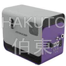
伯東公司代理日本 Atonarp 高科技分子傳感和數位診斷測試設備. Atonarp 通過結合先進的電子和數字處理演算法, 開創了化學成分分析領域的先河. 使高效, 經濟, 即時的獲取分子資訊成為現實! Atonarp 提供適用於半導體過程監控的 Aston™ 原位計量質譜分析儀
若您需要進一步的瞭解 Atonarp Aston™ 在線質譜儀詳細資訊或討論, 請參考以下聯絡方式:
上海伯東: 葉小姐 臺灣伯東: 王小姐
T: +86-21-5046-3511 ext 107 T: +886-3-567-9508 ext 161
F: +86-21-5046-1490 F: +886-3-567-0049
M: +86 1391-883-7267 ( 微信同號 ) M: +886-975-571-910
qq: 2821409400
現部分品牌誠招合作代理商, 有意向者歡迎聯絡伯東 王小姐 +886-975-571-910
伯東版權所有, 翻拷必究
![]() +886-2-8772-8910
+886-2-8772-8910